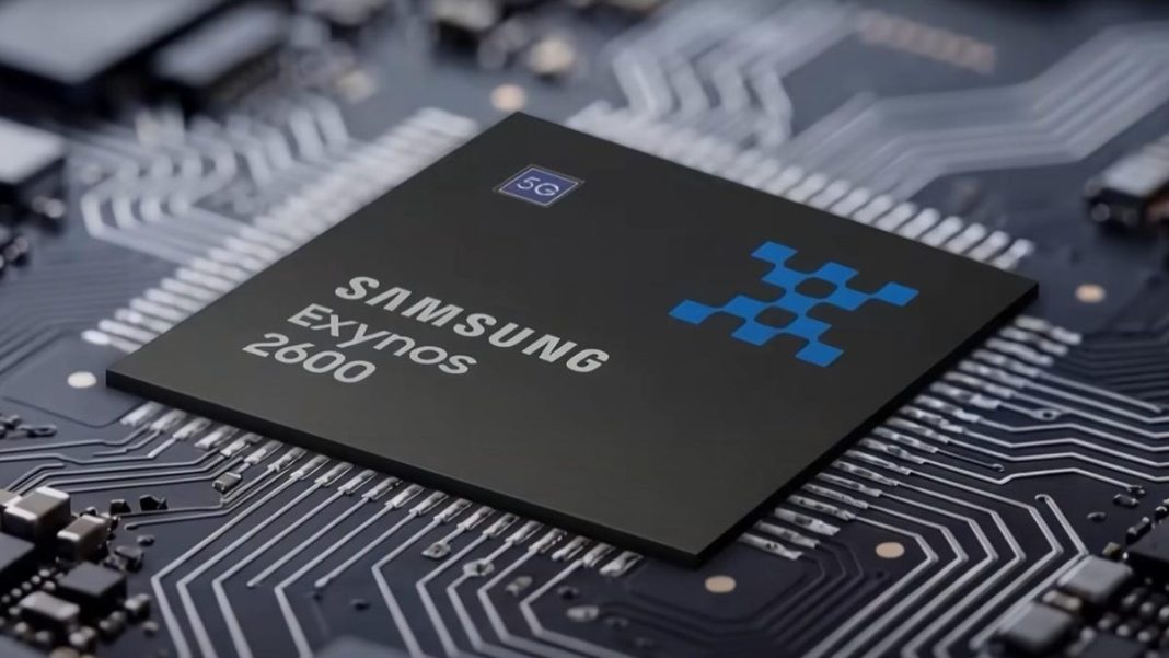
In the fiercely competitive Indian smartphone market, where consumers meticulously weigh every feature, the performance heart of a device – its processor – often dictates its success. Samsung, a dominant player, is not merely a smartphone manufacturer but also a formidable chipmaker through its foundry division. Recent breakthroughs in its semiconductor manufacturing process are poised to significantly impact its upcoming Galaxy phones, promising a leap forward that could redefine user expectations.
For years, the pursuit of smaller, more powerful, and energy-efficient chips has been the holy grail of the semiconductor industry. Samsung’s latest advancements, particularly in its 3-nanometer (nm) Gate-All-Around (GAA) process technology, represent a critical milestone. This isn’t just about incremental improvements; it’s a foundational shift that could unlock unprecedented capabilities for the next generation of Galaxy devices, from the flagship S-series to the foldable Z-series, and even influence its mid-range A-series offerings.
The Core of the Breakthrough: 3nm GAA Technology
The journey to smaller chip architecture has primarily relied on FinFET (Fin Field-Effect Transistor) technology. However, as chips shrink, the physical limitations of FinFET become apparent, leading to challenges in controlling current leakage and power consumption. Samsung’s move to 3nm GAA, specifically its Multi-Bridge-Channel FET (MBCFET) architecture, addresses these issues head-on. Unlike FinFET, where the gate only surrounds three sides of the channel, GAA transistors wrap the gate around all four sides of the channel. This allows for far superior control over the current flow.
What does this mean for your next Galaxy phone? Primarily, two critical benefits: significantly improved performance and drastically enhanced power efficiency. Industry estimates suggest that Samsung’s 3nm GAA process could deliver up to 23% higher performance and a remarkable 45% reduction in power consumption compared to its previous 5nm process, all while reducing the chip’s physical footprint by 16%. In the demanding Indian market, where users often juggle multiple apps, engage in graphics-intensive gaming, and consume high-definition multimedia, these gains translate directly into a smoother, more responsive, and longer-lasting user experience.
Transforming the Galaxy Experience: Beyond Raw Power
The implications of this chip breakthrough extend far beyond just faster app loading times. A more efficient and powerful processor acts as the bedrock for a multitude of advanced smartphone features:
Advanced AI and Computational Photography
Modern smartphone photography relies heavily on computational capabilities. With more powerful and efficient NPU (Neural Processing Unit) cores enabled by the new chip architecture, upcoming Galaxy phones can deliver even more sophisticated AI features. Imagine real-time language translation, more accurate on-device voice assistants, and groundbreaking advancements in camera processing – from superior low-light performance and noise reduction to more intelligent scene recognition and personalized photo enhancements. For Indian users, who are avid photographers and content creators, this means capturing stunning visuals with minimal effort.
Extended Battery Life and Optimized Thermals
Perhaps one of the most immediate and tangible benefits for everyday users is improved battery life. A 45% reduction in power consumption at the chip level is transformative. Even with more demanding features and always-on capabilities, users can expect their Galaxy phones to last significantly longer on a single charge. Furthermore, better efficiency also means less heat generation, leading to optimized thermal management. This is crucial for sustained performance during intense gaming sessions or prolonged video calls, ensuring the phone remains comfortable to hold and operates at peak efficiency without throttling.
As an industry expert recently noted, “Samsung’s 3nm GAA breakthrough isn’t just about winning the performance race; it’s about setting a new standard for smartphone efficiency and unlocking the next generation of AI-driven mobile experiences. This will be a significant differentiator in markets like India, where consumers demand both raw power and practical, day-long usability.”
Samsung’s Strategic Advantage in India and Globally
This semiconductor advancement also solidifies Samsung’s strategic position. As both a leading smartphone brand and a cutting-edge foundry, Samsung can directly integrate its best-in-class chip manufacturing capabilities into its own Exynos processors, potentially narrowing the performance gap with rivals like Qualcomm’s Snapdragon. It also positions Samsung Foundry as a more attractive partner for other tech giants seeking to manufacture their next-gen chips, further bolstering its ecosystem influence.
In the fiercely competitive Indian market, where Chinese brands and Apple constantly vie for market share, a robust, power-efficient, and feature-rich processor can be a decisive factor. Samsung’s ability to offer a truly differentiated experience, powered by its own groundbreaking silicon, could give its upcoming Galaxy phones a significant edge, catering to the evolving demands of Indian consumers who seek both innovation and practicality.
Ultimately, Samsung’s latest chip breakthrough is more than just a technical feat; it’s a promise of a smarter, faster, and more enduring mobile future. As these advanced processors make their way into upcoming Galaxy phones, Indian consumers can look forward to a new era of smartphone performance and efficiency that truly elevates their digital lives.


